An LED, a photodiode, and a measurement the ADC datasheet says you cannot make, on STM32F4 and ESP32-S3
Blink an LED at a carrier frequency, point it through the thing you want to measure, synchronously demodulate the photodiode current, and you have a photometer: a transmission or turbidity or colour-change instrument, the working core of a pulse oximeter, a smoke detector, a fluorometer. It is the best showcase the lock-in idea has on a microcontroller, because every hostile feature of the environment (sunlight, lamp flicker, amplifier drift, ADC noise) lands exactly where the main page showed the lock-in does not look.
The same theory that motivated the instrument also sizes it, before any hardware exists: the noise floor is \(\sqrt{S(f_0)/T}\) and nothing on the board can beat it, so the design starts from the formula and works outward. Both default platforms: NUCLEO-F446RE (Cortex-M4F) and ESP32-S3, single-precision float first.
The design, in numbers
Fix the operating point first; every code block below just implements it.
Sample rate\(f_s = 8\) kHz: comfortable for both ADCs, far above any carrier we need.
Carrier\(f_0 = f_s/9 \approx 888.9\) Hz: an exact rational fraction of the sample clock (9 samples per carrier cycle), above the 1/f corner of any reasonable front end, and deliberately not a multiple of 50 or 100 Hz, so no mains or lamp-flicker harmonic sits on top of it. The nearest line of the 50 Hz comb is 11.1 Hz away.
Block length\(N = 7200\) samples, \(T = 0.9\) s: a whole number of carrier cycles (800), so the coherent-integration condition from the previous topic holds exactly, and a whole number of 50 Hz mains cycles (45), which parks the entire mains comb on exact nulls of the block average.
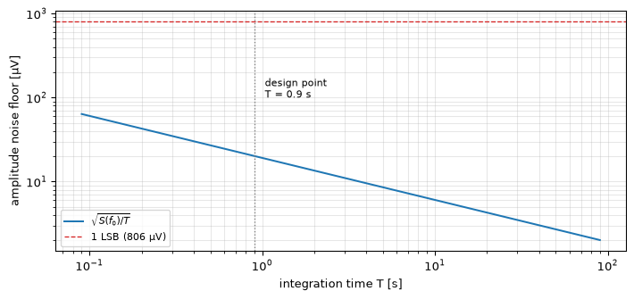
With the operating point fixed, the noise floor follows from one measured (or assumed, then measured) quantity: the total noise at the ADC input around the carrier frequency. Take a deliberately unflattering assumption, \(\sigma = 1.5\) LSB of a 12-bit converter on a 3.3 V range: noisier than either board’s converter needs to be at this bandwidth.
Show the code
fs, f0, N =8000.0, 8000.0/9.0, 7200T = N / fslsb =3.3/4096sigma =1.5* lsbS1 =2* sigma**2/ fs # one-sided PSD, V^2/HzTs = np.logspace(np.log10(0.09), np.log10(90), 60)floor = np.array([amplitude_noise_std(S1, t) for t in Ts])fig, ax = plt.subplots(figsize=(7.5, 3.6))ax.loglog(Ts, floor *1e6, 'C0', lw=1.5, label=r'$\sqrt{S(f_0)/T}$')ax.axhline(lsb *1e6, color='C3', ls='--', lw=1, label='1 LSB (806 µV)')ax.axvline(T, color='gray', ls=':', lw=1)ax.annotate(f'design point\nT = {T} s', (T *1.15, 100), fontsize=8)ax.set_xlabel('integration time T [s]')ax.set_ylabel('amplitude noise floor [µV]')ax.legend(fontsize=8); ax.grid(True, which='both', alpha=0.3)fig.tight_layout(); plt.show()sig = amplitude_noise_std(S1, T)print(f"LSB = {lsb*1e3:.4f} mV, sigma = {sigma*1e3:.4f} mV")print(f"floor at T = {T} s: {sig*1e6:.1f} uV = {sig/lsb:.4f} LSB")print(f"blocks per second: {fs/N:.2f}, carrier cycles per block: {f0*N/fs:.0f}, "f"mains cycles per block: {50*T:.0f}")assertabs(sig - sigma * np.sqrt(2/ N)) <1e-12# same formula, two routesassert19e-6< sig <21e-6, "the quoted 20 uV floor"assert sig / lsb <0.03, "comfortably sub-LSB"assert f0 * N / fs ==800and50* T ==45, "whole cycles of carrier AND mains"
Figure 1: The photometer’s noise floor against integration time, from var(Â) = 2σ²/N with σ = 1.5 LSB of a 12-bit, 3.3 V ADC. At the design point T = 0.9 s the floor is 20 µV, about 0.025 LSB: a fortieth of the quantisation step, measured through the quantiser. Longer blocks keep buying at the white-noise rate because the carrier sits above the front end’s 1/f corner: that is the main page’s whole argument, cashed in.
LSB = 0.8057 mV, sigma = 1.2085 mV
floor at T = 0.9 s: 20.1 uV = 0.0250 LSB
blocks per second: 1.11, carrier cycles per block: 800, mains cycles per block: 45
Read the design point off the plot: 20 µV in 0.9 s, a fortieth of the ADC step, and every octave of patience halves the variance. If the photodiode signal at the ADC is, say, 100 mV of carrier amplitude, that is a 1-in-5000 transmission measurement per second from a 12-bit converter, which is why this instrument is such a satisfying build.
Sub-LSB honesty: the dither clause
Resolving 0.025 LSB through a quantiser leans on a condition: the total noise at the converter must be at least on the order of one LSB, so that quantisation behaves as noise rather than as a deterministic staircase. That is the dither page’s core result, and it is why the unflattering σ = 1.5 LSB assumption above is not a pessimism to apologise for but a requirement. The archive slide quoted on the main page (“dithering is accomplished by interference”) makes the same point from 2007: ambient light and front-end noise are the free dither that linearises the measurement. A front end so clean that the ADC reading never toggles would actually break the sub-LSB claim; see the ADC-noise page for the oversampling arithmetic.
One clock, three frequencies
Everything above assumed \(f_0/f_s\) is exactly\(1/9\) and the block is exactly 800 cycles. That is a statement about clock tree design, not arithmetic: derive the LED drive and the ADC trigger from the same timebase and the ratio is exact by construction, forever, with any crystal error cancelling in the ratio. Get this right and the phase reading is a constant; get it wrong (LED from a free-running RC oscillator, say) and the carrier slides through the demodulation window.
How much slide is tolerable? A frequency error \(\delta f\) costs amplitude by the same leakage mechanism as any off-bin tone, a factor \(|\mathrm{sinc}(\delta f\, T)|\), and it costs it quadratically, so small errors are forgiving:
Show the code
# Tolerance budget for the design point, from sinc(df*T), plus the# mains-comb rejection the 0.9 s block buys.from numpy import sinc # normalised: sinc(x) = sin(pi x)/(pi x)for df in (0.01, 0.05, 0.1, 0.5): loss =1-abs(sinc(df * T))print(f"carrier error {df:5.2f} Hz ({df/f0*1e6:6.0f} ppm): "f"amplitude loss {loss*100:.2f}%")# Mains comb: on-frequency mains lands on exact nulls (whole cycles);# with the mains fundamental off by 0.05 Hz, the k-th harmonic sits# k*0.05 Hz off its null and the sidelobe envelope 1/(pi*df*T) applies# around the nearest comb line, 11.1 Hz from the carrier.df_comb =900.0- f0 # nearest 50 Hz harmonic offsetworst =1/ (np.pi * (df_comb -18*0.05) * T)print(f"nearest mains line: {df_comb:.1f} Hz away; worst-case rejection "f"with 50 Hz off by 0.05 Hz: {20*np.log10(worst):.0f} dB")assertabs(sinc(0.05* T)) >0.996, "50 mHz carrier error costs under 0.4%"assert1-abs(sinc(0.5* T)) >0.25, "500 mHz costs real amplitude"assert20* np.log10(worst) <-29, "at least ~30 dB against a wandering comb"
carrier error  0.01 Hz (    11 ppm): amplitude loss 0.01%
carrier error  0.05 Hz (    56 ppm): amplitude loss 0.33%
carrier error  0.10 Hz (   112 ppm): amplitude loss 1.33%
carrier error  0.50 Hz (   562 ppm): amplitude loss 30.14%
nearest mains line: 11.1 Hz away; worst-case rejection with 50 Hz off by 0.05 Hz: -29 dB
Three numbers to carry into the wiring: a carrier error of 50 mHz (56 ppm) is free, and anything derived from one crystal is orders of magnitude inside that; the mains comb sits on exact nulls when the grid is on frequency; and even with the grid off by 0.05 Hz the geometry still buys about 30 dB, before the optics’ own flicker rolloff and any analogue filtering. This layered rejection, distance from the comb plus nulls on the comb, is why \(f_0\) and \(T\) were chosen together rather than independently.
The portable core
The demodulator is small enough to state completely. Because \(f_0/f_s = 1/9\), the reference repeats every 9 samples: one 9-entry quadrature table, two multiply-accumulates per sample, no buffer at all. Compare the tone tracker’s FFT path (kilobytes of RAM, thousands of flops per block): knowing the frequency is worth that much.
#include <math.h>#include <stdint.h>#define M_REF 9/* samples per carrier cycle */#define N_BLOCK 7200/* 800 carrier cycles = 0.9 s */staticfloat ref_cos[M_REF], ref_sin[M_REF];void lockin_init(void){for(int k =0; k < M_REF; k++){ ref_cos[k]= cosf(2.0f*(float)M_PI * k / M_REF); ref_sin[k]= sinf(2.0f*(float)M_PI * k / M_REF);}}/* Feed every ADC sample; returns 1 when a block result is ready. */typedefstruct{float i, q;uint32_t n;} lockin_acc_t;staticint lockin_push(lockin_acc_t *acc,float x,float*amplitude,float*phase){uint32_t k = acc->n % M_REF; acc->i += x * ref_cos[k]; acc->q -= x * ref_sin[k];if(++acc->n < N_BLOCK)return0;/* Single-bin DFT bookkeeping: 2/N recovers the amplitude of A*cos(2*pi*f0*t + phi); see the main page. */float zi =2.0f* acc->i /(float)N_BLOCK;float zq =2.0f* acc->q /(float)N_BLOCK;*amplitude = sqrtf(zi * zi + zq * zq);*phase = atan2f(zq, zi); acc->i = acc->q =0.0f; acc->n =0;return1;}
Two properties matter and both come from the whole-cycles design. The DC component of the input, which for a photometer is ambient light plus the LED’s average level and can dwarf the carrier, sums to exactly zero against both reference tables over a block: ambient rejection is built into the arithmetic before any analogue filter is asked for. And the magnitude/phase output means the LED timer and the ADC timer may start in any relative alignment: the phase reading will differ, the amplitude will not. Only the frequency ratio must be exact, which the wiring below guarantees.
One bookkeeping constant remains: the LED is driven on/off (a square), so the optical carrier’s fundamental is \(\tfrac{2}{\pi}\) of the on-amplitude (the square wave’s \(\tfrac{4}{\pi}\) harmonic coefficient times the half-depth), as derived on the main page. Fold it, the transimpedance gain, and the LED power into one end-to-end calibration factor and measure that factor once against a known target; do not stack datasheet numbers.
On the STM32F4 (NUCLEO-F446RE)
The clock chain is the design. Both TIM3 and TIM4 sit on the same internal timer bus; give both the same prescaler so they count the same 1 MHz timebase, then let TIM3 (period 125 ticks → 8 kHz) trigger the ADC while TIM4 (period 1125 ticks, 50% compare → 888.89 Hz) drives the LED. \(1125 = 9 \times 125\), so \(f_0 = f_s/9\)exactly, in hardware, with no software in the loop.
#include "stm32f4xx_hal.h"/* TIM3: ADC trigger at 8 kHz. TIM4: LED PWM at fs/9. Same prescaler on the same timer bus => exact 1:9 ratio. */void photometer_timers_init(TIM_HandleTypeDef *tim3, TIM_HandleTypeDef *tim4,uint32_t timer_bus_hz){uint32_t presc = timer_bus_hz /1000000u-1u;/* 1 MHz timebase */ tim3->Init.Prescaler = presc; tim3->Init.Period =125u-1u;/* 8 kHz */ HAL_TIM_Base_Init(tim3);/* Route TIM3's update event to TRGO: this IS the ADC trigger. The ADC must be configured to listen for it, with ExternalTrigConv = ADC_EXTERNALTRIGCONV_T3_TRGO. */ TIM_MasterConfigTypeDef ms ={0}; ms.MasterOutputTrigger = TIM_TRGO_UPDATE; HAL_TIMEx_MasterConfigSynchronization(tim3,&ms); tim4->Init.Prescaler = presc; tim4->Init.Period =1125u-1u;/* 888.889 Hz */ HAL_TIM_PWM_Init(tim4); TIM_OC_InitTypeDef oc ={0}; oc.OCMode = TIM_OCMODE_PWM1; oc.Pulse =562u;/* ~50% duty */ HAL_TIM_PWM_ConfigChannel(tim4,&oc, TIM_CHANNEL_1);/* Start the LED first, then the trigger source; call HAL_ADC_Start_DMA() before this function so no trigger is lost. */ HAL_TIM_PWM_Start(tim4, TIM_CHANNEL_1); HAL_TIM_Base_Start(tim3);}/* ADC in DMA circular mode, half/full-transfer callbacks feeding the demodulator; buffer sized in samples, far smaller than a block. */#define DMA_CHUNK 288/* 32 carrier cycles */staticuint16_t adc_buf[2* DMA_CHUNK];static lockin_acc_t acc;staticvoid process(constuint16_t*s){float amplitude, phase;for(int n =0; n < DMA_CHUNK; n++)if(lockin_push(&acc,(float)s[n]*(3.3f/4096.0f),&litude,&phase)) photometer_report(amplitude, phase);/* once per 0.9 s */}void HAL_ADC_ConvHalfCpltCallback(ADC_HandleTypeDef *h){ process(adc_buf);}void HAL_ADC_ConvCpltCallback(ADC_HandleTypeDef *h){ process(adc_buf + DMA_CHUNK);}
The DMA_CHUNK of 288 samples is a whole number of carrier cycles (32), which keeps each callback’s contribution to the accumulators self-contained; any multiple of 9 works. Per sample the demodulator is two multiplies and two adds against an 18-float table: at 8 kHz this rounds to zero load on a 180 MHz M4F, and there is no cycle-budget table here because nothing about this design is near a budget. Measure with DWT->CYCCNT if you extend it.
On the ESP32-S3
The same design maps onto ESP-IDF with two peripherals: continuous-mode ADC (DMA) for sampling, and a GPTimer callback toggling the LED GPIO. Both derive from the same 40 MHz crystal, so the frequency ratio is again fixed by dividers, not by luck: the GPTimer below resolves 10 MHz and toggles every 5625 ticks, giving \(10\,\text{MHz}/(2 \times 5625) = 888.889\) Hz against the ADC’s 8 kHz, the exact \(f_s/9\) once more.
One honest caveat separates this from the STM32 path. There, a single prescaler feeds both timers and the 1:9 ratio is structurally exact. Here, two driver stacks each compute their own dividers from the same crystal; the chosen numbers divide evenly on paper (10 MHz and 8 kHz both divide the ADC framework’s clocks), but the drivers do not promise it. So verify coherence the way an instrument engineer would, using the lock-in itself: watch the phase output over minutes. A fixed clock-tree ratio shows as a constant phase; a divider rounding error of \(\delta f\) shows as phase advancing at \(2\pi\,\delta f\) radians per second, and the timing-budget cell above says anything below 50 mHz of drift is costing you under half a percent. If it drifts more, adjust TOGGLE_TICKS by the measured amount: a lock-in is its own frequency counter, which is the kind of bootstrap that makes this instrument fun.
The front end: from photocurrent to ADC volts
The electronics ask is modest, one op-amp, because the lock-in tolerates everything a fancier front end would fix. A photodiode into a transimpedance amplifier gives \(V = I_{pd} R_f\): with a few µA of photocurrent and \(R_f = 100\) kΩ, hundreds of millivolts of carrier at the ADC (example values; size \(R_f\) from your diode and geometry). Two checks, both from the design point rather than from habit:
Bandwidth: the TIA needs to pass 889 Hz. Its pole sits at \(1/(2\pi R_f C)\) with \(C\) the diode-plus-feedback capacitance; at 100 kΩ that allows tens of picofarads with an order of magnitude to spare. The lock-in needs no bandwidth beyond the carrier: rolloff above \(f_0\) is free anti-alias filtering.
Headroom, not filtering, for ambient light: direct sunlight can push a photodiode’s DC current far above the signal. The demodulator rejects DC exactly, but only if the front end has not clipped first: the dynamic-range budget goes to keeping the ambient pedestal inside the rails, by AC coupling after the TIA, by a smaller \(R_f\), or by optics. This is the 2007 archive deck’s dynamic-range lesson in miniature, and it is also exactly how PPG sensor modules work: the MAX30102 of the PPG topic pulses its LEDs and samples ambient between pulses, a time-domain cousin of this frequency-domain rejection.
From the archive: the charge-integrating alternative, 2008
The second archive deck behind this topic treats photodiode readout for very small currents, where a resistor big enough to develop signal voltage would be noisy and slow. Its front end is a resettable charge integrator: dump the photocurrent into a capacitor for an integration window, \(V = I\,T_{int}/C\) (a gain of \(T_{int}/C\) volts per ampere), sample, reset, repeat. Its two design facts: the transfer averages the current over the window, giving the same \(\mathrm{sinc}\) rolloff as any block average (the deck: “a resettable integrator equals a sample-and-hold, transfer almost ideal first-order low-pass”); and each reset leaves \(kT/C\) noise on the capacitor, because at reset the switch and capacitor reach thermal equilibrium, \(\tfrac{1}{2}C\,\overline{v_n^2} = \tfrac{1}{2}kT\). The deck’s memorable framing is that a switched capacitor is a resistor of \(R_{eq} = 1/(f_s C)\), noise included, since it moves charge \(Q = CV\) once per period, so \(I = C V f_s\).
Show the code
# The 2008 deck's numbers.kB, T_room =1.380649e-23, 300.0C =10e-12# the deck's 10 pF examplefs_ci =17.6e3# and its 17.6 kSpsv_reset = np.sqrt(kB * T_room / C)R_eq =1/ (fs_ci * C)gain = (1/ fs_ci) / C # V per A if T_int spans the periodprint(f"kT/C reset noise at 10 pF: {v_reset*1e6:.1f} uV rms")print(f"switched-cap equivalent resistance: {R_eq/1e6:.2f} MOhm")print(f"charge-integrator gain at T_int = 1/fs: {gain:.3g} V/A")assert19e-6< v_reset <21e-6# ~20 uVassert5.5e6< R_eq <6.0e6# ~5.7 MOhm
kT/C reset noise at 10 pF: 20.4 uV rms
switched-cap equivalent resistance: 5.68 MOhm
charge-integrator gain at T_int = 1/fs: 5.68e+06 V/A
Worth noticing: 20 µV of reset noise per sample, and the photometer’s demodulated floor was also 20 µV, from noise 60 times larger. The lock-in’s averaging is doing for the cheap front end what exotic electronics would otherwise have to do alone.
When there is no FPU
The core is friendlier to integer machines than almost any DSP block in this workshop. Keep the ADC samples as int32_t, scale the 9-entry reference table to Q15 (ref_q15[k] = lroundf(32767 * cosf(...))), and accumulate x * ref_q15[k] into an int64_t: at 12 input bits, 15 coefficient bits, and \(N = 7200\) samples the accumulator peaks near \(2^{40}\), decades inside 64-bit range, so no per-stage scaling is needed at all, the trap that makes fixed-point FFTs hard (finite word-length effects) simply never arises. One square root and one arctangent per 0.9 s remain in software float, at a cost of nothing. An ATmega328P could run this instrument; the capability-ladder lesson is that the lock-in’s arithmetic was never the hard part, the clock discipline was.
References
Source Code
---title: "A Lock-in Photometer on Hardware"subtitle: "An LED, a photodiode, and a measurement the ADC datasheet says you cannot make, on STM32F4 and ESP32-S3"description-meta: "An LED, a photodiode and synchronous demodulation on the STM32F4 and ESP32-S3: a photometer that measures below the ADC noise floor."bibliography: ../../references.bib---Blink an LED at a carrier frequency, point it through the thing you want to measure, synchronously demodulate the photodiode current, and you have a **photometer**: a transmission or turbidity or colour-change instrument, the working core of a pulse oximeter, a smoke detector, a fluorometer. It is the best showcase the lock-in idea has on a microcontroller, because every hostile feature of the environment (sunlight, lamp flicker, amplifier drift, ADC noise) lands exactly where [the main page](index.qmd) showed the lock-in does not look.The same theory that motivated the instrument also *sizes* it, before any hardware exists: the noise floor is $\sqrt{S(f_0)/T}$ and nothing on the board can beat it, so the design starts from the formula and works outward. Both default platforms: NUCLEO-F446RE (Cortex-M4F) and ESP32-S3, single-precision `float` first.```{python}#| echo: falseimport numpy as npimport matplotlib.pyplot as pltfrom lockin import amplitude_noise_std, enbw```<hr>## The design, in numbersFix the operating point first; every code block below just implements it.- **Sample rate** $f_s = 8$ kHz: comfortable for both ADCs, far above any carrier we need.- **Carrier** $f_0 = f_s/9 \approx 888.9$ Hz: an exact rational fraction of the sample clock (9 samples per carrier cycle), above the 1/f corner of any reasonable front end, and deliberately *not* a multiple of 50 or 100 Hz, so no mains or lamp-flicker harmonic sits on top of it. The nearest line of the 50 Hz comb is 11.1 Hz away.- **Block length** $N = 7200$ samples, $T = 0.9$ s: a whole number of carrier cycles (800), so the coherent-integration condition from [the previous topic](../estimating-a-sinusoid/index.qmd#known-frequency-the-coherent-single-bin-dft) holds exactly, *and* a whole number of 50 Hz mains cycles (45), which parks the entire mains comb on exact nulls of the block average.With the operating point fixed, the noise floor follows from one measured (or assumed, then measured) quantity: the total noise at the ADC input around the carrier frequency. Take a deliberately unflattering assumption, $\sigma = 1.5$ LSB of a 12-bit converter on a 3.3 V range: noisier than either board's converter needs to be at this bandwidth.```{python}#| label: fig-sizing#| fig-cap: "The photometer's noise floor against integration time, from var(Â) = 2σ²/N with σ = 1.5 LSB of a 12-bit, 3.3 V ADC. At the design point T = 0.9 s the floor is 20 µV, about 0.025 LSB: a fortieth of the quantisation step, measured through the quantiser. Longer blocks keep buying at the white-noise rate because the carrier sits above the front end's 1/f corner: that is the main page's whole argument, cashed in."fs, f0, N =8000.0, 8000.0/9.0, 7200T = N / fslsb =3.3/4096sigma =1.5* lsbS1 =2* sigma**2/ fs # one-sided PSD, V^2/HzTs = np.logspace(np.log10(0.09), np.log10(90), 60)floor = np.array([amplitude_noise_std(S1, t) for t in Ts])fig, ax = plt.subplots(figsize=(7.5, 3.6))ax.loglog(Ts, floor *1e6, 'C0', lw=1.5, label=r'$\sqrt{S(f_0)/T}$')ax.axhline(lsb *1e6, color='C3', ls='--', lw=1, label='1 LSB (806 µV)')ax.axvline(T, color='gray', ls=':', lw=1)ax.annotate(f'design point\nT = {T} s', (T *1.15, 100), fontsize=8)ax.set_xlabel('integration time T [s]')ax.set_ylabel('amplitude noise floor [µV]')ax.legend(fontsize=8); ax.grid(True, which='both', alpha=0.3)fig.tight_layout(); plt.show()sig = amplitude_noise_std(S1, T)print(f"LSB = {lsb*1e3:.4f} mV, sigma = {sigma*1e3:.4f} mV")print(f"floor at T = {T} s: {sig*1e6:.1f} uV = {sig/lsb:.4f} LSB")print(f"blocks per second: {fs/N:.2f}, carrier cycles per block: {f0*N/fs:.0f}, "f"mains cycles per block: {50*T:.0f}")assertabs(sig - sigma * np.sqrt(2/ N)) <1e-12# same formula, two routesassert19e-6< sig <21e-6, "the quoted 20 uV floor"assert sig / lsb <0.03, "comfortably sub-LSB"assert f0 * N / fs ==800and50* T ==45, "whole cycles of carrier AND mains"```Read the design point off the plot: **20 µV in 0.9 s**, a fortieth of the ADC step, and every octave of patience halves the variance. If the photodiode signal at the ADC is, say, 100 mV of carrier amplitude, that is a 1-in-5000 transmission measurement per second from a 12-bit converter, which is why this instrument is such a satisfying build.::: {.callout-warning title="Sub-LSB honesty: the dither clause"}Resolving 0.025 LSB *through a quantiser* leans on a condition: the total noise at the converter must be at least on the order of one LSB, so that quantisation behaves as noise rather than as a deterministic staircase. That is the [dither page's](../dither/index.qmd) core result, and it is why the unflattering σ = 1.5 LSB assumption above is not a pessimism to apologise for but a *requirement*. The archive slide quoted on the main page ("dithering is accomplished by interference") makes the same point from 2007: ambient light and front-end noise are the free dither that linearises the measurement. A front end so clean that the ADC reading never toggles would actually *break* the sub-LSB claim; see the [ADC-noise page](../adc-noise/index.qmd) for the oversampling arithmetic.:::<hr>## One clock, three frequenciesEverything above assumed $f_0/f_s$ is *exactly* $1/9$ and the block is *exactly* 800 cycles. That is a statement about clock tree design, not arithmetic: derive the LED drive and the ADC trigger from the same timebase and the ratio is exact by construction, forever, with any crystal error cancelling in the ratio. Get this right and the phase reading is a constant; get it wrong (LED from a free-running RC oscillator, say) and the carrier slides through the demodulation window.How much slide is tolerable? A frequency error $\delta f$ costs amplitude by the same leakage mechanism as any off-bin tone, a factor $|\mathrm{sinc}(\delta f\, T)|$, and it costs it quadratically, so small errors are forgiving:```{python}#| label: timing-budget# Tolerance budget for the design point, from sinc(df*T), plus the# mains-comb rejection the 0.9 s block buys.from numpy import sinc # normalised: sinc(x) = sin(pi x)/(pi x)for df in (0.01, 0.05, 0.1, 0.5): loss =1-abs(sinc(df * T))print(f"carrier error {df:5.2f} Hz ({df/f0*1e6:6.0f} ppm): "f"amplitude loss {loss*100:.2f}%")# Mains comb: on-frequency mains lands on exact nulls (whole cycles);# with the mains fundamental off by 0.05 Hz, the k-th harmonic sits# k*0.05 Hz off its null and the sidelobe envelope 1/(pi*df*T) applies# around the nearest comb line, 11.1 Hz from the carrier.df_comb =900.0- f0 # nearest 50 Hz harmonic offsetworst =1/ (np.pi * (df_comb -18*0.05) * T)print(f"nearest mains line: {df_comb:.1f} Hz away; worst-case rejection "f"with 50 Hz off by 0.05 Hz: {20*np.log10(worst):.0f} dB")assertabs(sinc(0.05* T)) >0.996, "50 mHz carrier error costs under 0.4%"assert1-abs(sinc(0.5* T)) >0.25, "500 mHz costs real amplitude"assert20* np.log10(worst) <-29, "at least ~30 dB against a wandering comb"```Three numbers to carry into the wiring: a carrier error of **50 mHz (56 ppm) is free**, and anything derived from one crystal is orders of magnitude inside that; the mains comb sits on **exact nulls** when the grid is on frequency; and even with the grid off by 0.05 Hz the geometry still buys about **30 dB**, *before* the optics' own flicker rolloff and any analogue filtering. This layered rejection, distance from the comb plus nulls on the comb, is why $f_0$ and $T$ were chosen together rather than independently.<hr>## The portable coreThe demodulator is small enough to state completely. Because $f_0/f_s = 1/9$, the reference repeats every 9 samples: one 9-entry quadrature table, two multiply-accumulates per sample, no buffer at all. Compare the [tone tracker's](../estimating-a-sinusoid/embedded.qmd) FFT path (kilobytes of RAM, thousands of flops per block): *knowing the frequency* is worth that much.```c#include <math.h>#include <stdint.h>#define M_REF 9/* samples per carrier cycle */#define N_BLOCK 7200/* 800 carrier cycles = 0.9 s */staticfloat ref_cos[M_REF], ref_sin[M_REF];void lockin_init(void){for(int k =0; k < M_REF; k++){ ref_cos[k]= cosf(2.0f*(float)M_PI * k / M_REF); ref_sin[k]= sinf(2.0f*(float)M_PI * k / M_REF);}}/* Feed every ADC sample; returns 1 when a block result is ready. */typedefstruct{float i, q;uint32_t n;} lockin_acc_t;staticint lockin_push(lockin_acc_t *acc,float x,float*amplitude,float*phase){uint32_t k = acc->n % M_REF; acc->i += x * ref_cos[k]; acc->q -= x * ref_sin[k];if(++acc->n < N_BLOCK)return0;/* Single-bin DFT bookkeeping: 2/N recovers the amplitude of A*cos(2*pi*f0*t + phi); see the main page. */float zi =2.0f* acc->i /(float)N_BLOCK;float zq =2.0f* acc->q /(float)N_BLOCK;*amplitude = sqrtf(zi * zi + zq * zq);*phase = atan2f(zq, zi); acc->i = acc->q =0.0f; acc->n =0;return1;}```Two properties matter and both come from the whole-cycles design. The DC component of the input, which for a photometer is *ambient light plus the LED's average level* and can dwarf the carrier, sums to exactly zero against both reference tables over a block: ambient rejection is built into the arithmetic before any analogue filter is asked for. And the magnitude/phase output means the LED timer and the ADC timer may start in any relative alignment: the phase reading will differ, the amplitude will not. Only the *frequency* ratio must be exact, which the wiring below guarantees.One bookkeeping constant remains: the LED is driven on/off (a square), so the optical carrier's fundamental is $\tfrac{2}{\pi}$ of the on-amplitude (the square wave's $\tfrac{4}{\pi}$ harmonic coefficient times the half-depth), as derived [on the main page](index.qmd#the-square-wave-reference-a-cheap-trick-and-its-exact-price). Fold it, the transimpedance gain, and the LED power into one end-to-end calibration factor and measure that factor once against a known target; do not stack datasheet numbers.<hr>## On the STM32F4 (NUCLEO-F446RE)The clock chain is the design. Both TIM3 and TIM4 sit on the same internal timer bus; give both the same prescaler so they count the same 1 MHz timebase, then let TIM3 (period 125 ticks → 8 kHz) trigger the ADC while TIM4 (period 1125 ticks, 50% compare → 888.89 Hz) drives the LED. $1125 = 9 \times 125$, so $f_0 = f_s/9$ *exactly*, in hardware, with no software in the loop.```c#include "stm32f4xx_hal.h"/* TIM3: ADC trigger at 8 kHz. TIM4: LED PWM at fs/9. Same prescaler on the same timer bus => exact 1:9 ratio. */void photometer_timers_init(TIM_HandleTypeDef *tim3, TIM_HandleTypeDef *tim4,uint32_t timer_bus_hz){uint32_t presc = timer_bus_hz /1000000u-1u;/* 1 MHz timebase */ tim3->Init.Prescaler = presc; tim3->Init.Period =125u-1u;/* 8 kHz */ HAL_TIM_Base_Init(tim3);/* Route TIM3's update event to TRGO: this IS the ADC trigger. The ADC must be configured to listen for it, with ExternalTrigConv = ADC_EXTERNALTRIGCONV_T3_TRGO. */ TIM_MasterConfigTypeDef ms ={0}; ms.MasterOutputTrigger = TIM_TRGO_UPDATE; HAL_TIMEx_MasterConfigSynchronization(tim3,&ms); tim4->Init.Prescaler = presc; tim4->Init.Period =1125u-1u;/* 888.889 Hz */ HAL_TIM_PWM_Init(tim4); TIM_OC_InitTypeDef oc ={0}; oc.OCMode = TIM_OCMODE_PWM1; oc.Pulse =562u;/* ~50% duty */ HAL_TIM_PWM_ConfigChannel(tim4,&oc, TIM_CHANNEL_1);/* Start the LED first, then the trigger source; call HAL_ADC_Start_DMA() before this function so no trigger is lost. */ HAL_TIM_PWM_Start(tim4, TIM_CHANNEL_1); HAL_TIM_Base_Start(tim3);}/* ADC in DMA circular mode, half/full-transfer callbacks feeding the demodulator; buffer sized in samples, far smaller than a block. */#define DMA_CHUNK 288/* 32 carrier cycles */staticuint16_t adc_buf[2* DMA_CHUNK];static lockin_acc_t acc;staticvoid process(constuint16_t*s){float amplitude, phase;for(int n =0; n < DMA_CHUNK; n++)if(lockin_push(&acc,(float)s[n]*(3.3f/4096.0f),&litude,&phase)) photometer_report(amplitude, phase);/* once per 0.9 s */}void HAL_ADC_ConvHalfCpltCallback(ADC_HandleTypeDef *h){ process(adc_buf);}void HAL_ADC_ConvCpltCallback(ADC_HandleTypeDef *h){ process(adc_buf + DMA_CHUNK);}```The `DMA_CHUNK` of 288 samples is a whole number of carrier cycles (32), which keeps each callback's contribution to the accumulators self-contained; any multiple of 9 works. Per sample the demodulator is two multiplies and two adds against an 18-float table: at 8 kHz this rounds to zero load on a 180 MHz M4F, and there is no cycle-budget table here because nothing about this design is near a budget. Measure with `DWT->CYCCNT` if you extend it.<hr>## On the ESP32-S3The same design maps onto ESP-IDF with two peripherals: continuous-mode ADC (DMA) for sampling, and a GPTimer callback toggling the LED GPIO. Both derive from the same 40 MHz crystal, so the frequency *ratio* is again fixed by dividers, not by luck: the GPTimer below resolves 10 MHz and toggles every 5625 ticks, giving $10\,\text{MHz}/(2 \times 5625) = 888.889$ Hz against the ADC's 8 kHz, the exact $f_s/9$ once more.```c#include "driver/gptimer.h"#include "driver/gpio.h"#include "esp_adc/adc_continuous.h"#define LED_GPIO 4#define FS_HZ 8000#define TOGGLE_TICKS 5625u/* 10 MHz / (2 * 5625) = 888.889 Hz */staticbool IRAM_ATTR led_toggle_cb(gptimer_handle_t t,const gptimer_alarm_event_data_t *e,void*arg){staticuint32_t level =0; gpio_set_level(LED_GPIO, level ^=1u);returnfalse;}void photometer_led_init(void){ gptimer_handle_t timer; gptimer_config_t cfg ={.clk_src = GPTIMER_CLK_SRC_DEFAULT,.direction = GPTIMER_COUNT_UP,.resolution_hz =10*1000*1000,}; gptimer_new_timer(&cfg,&timer); gptimer_alarm_config_t alarm ={.alarm_count = TOGGLE_TICKS,.flags.auto_reload_on_alarm =true,}; gptimer_set_alarm_action(timer,&alarm); gptimer_event_callbacks_t cbs ={.on_alarm = led_toggle_cb }; gptimer_register_event_callbacks(timer,&cbs, NULL); gptimer_enable(timer); gptimer_start(timer);}```The sampling side uses continuous-mode ADC through DMA, with a reader task playing the role of the STM32's DMA callbacks:```c#include "freertos/FreeRTOS.h"#include "freertos/task.h"#include "esp_adc/adc_continuous.h"#define FRAME_SAMPLES 288/* 32 carrier cycles per frame */#define FRAME_BYTES (FRAME_SAMPLES * SOC_ADC_DIGI_RESULT_BYTES)static adc_continuous_handle_t adc;static lockin_acc_t acc;void photometer_adc_init(void){ adc_continuous_handle_cfg_t hcfg ={.max_store_buf_size =4* FRAME_BYTES,.conv_frame_size = FRAME_BYTES,}; adc_continuous_new_handle(&hcfg,&adc); adc_digi_pattern_config_t pattern ={.atten = ADC_ATTEN_DB_12,.channel = ADC_CHANNEL_3,/* the photodiode input */.unit = ADC_UNIT_1,.bit_width = ADC_BITWIDTH_12,}; adc_continuous_config_t ccfg ={.pattern_num =1,.adc_pattern =&pattern,.sample_freq_hz = FS_HZ,.conv_mode = ADC_CONV_SINGLE_UNIT_1,.format = ADC_DIGI_OUTPUT_FORMAT_TYPE2,}; adc_continuous_config(adc,&ccfg); adc_continuous_start(adc);}void photometer_task(void*arg){staticuint8_t frame[FRAME_BYTES];uint32_t got;float amplitude, phase;for(;;){if(adc_continuous_read(adc, frame,sizeof frame,&got, portMAX_DELAY)!= ESP_OK)continue; adc_digi_output_data_t *p =(adc_digi_output_data_t *)frame;for(uint32_t n =0; n < got / SOC_ADC_DIGI_RESULT_BYTES; n++)/* Nominal volts-per-count; the end-to-end calibration factor absorbs the attenuator's real full scale. */if(lockin_push(&acc,(float)p[n].type2.data *(3.3f/4096.0f),&litude,&phase)) photometer_report(amplitude, phase);}}```One honest caveat separates this from the STM32 path. There, a single prescaler feeds both timers and the 1:9 ratio is *structurally* exact. Here, two driver stacks each compute their own dividers from the same crystal; the chosen numbers divide evenly on paper (10 MHz and 8 kHz both divide the ADC framework's clocks), but the drivers do not promise it. So verify coherence the way an instrument engineer would, using the lock-in itself: watch the **phase** output over minutes. A fixed clock-tree ratio shows as a constant phase; a divider rounding error of $\delta f$ shows as phase advancing at $2\pi\,\delta f$ radians per second, and the timing-budget cell above says anything below 50 mHz of drift is costing you under half a percent. If it drifts more, adjust `TOGGLE_TICKS` by the measured amount: a lock-in is its own frequency counter, which is the kind of bootstrap that makes this instrument fun.<hr>## The front end: from photocurrent to ADC voltsThe electronics ask is modest, one op-amp, because the lock-in tolerates everything a fancier front end would fix. A photodiode into a transimpedance amplifier gives $V = I_{pd} R_f$: with a few µA of photocurrent and $R_f = 100$ kΩ, hundreds of millivolts of carrier at the ADC (example values; size $R_f$ from your diode and geometry). Two checks, both from the design point rather than from habit:- **Bandwidth**: the TIA needs to pass 889 Hz. Its pole sits at $1/(2\pi R_f C)$ with $C$ the diode-plus-feedback capacitance; at 100 kΩ that allows tens of picofarads with an order of magnitude to spare. The lock-in needs no bandwidth *beyond* the carrier: rolloff above $f_0$ is free anti-alias filtering.- **Headroom, not filtering, for ambient light**: direct sunlight can push a photodiode's DC current far above the signal. The demodulator rejects DC *exactly*, but only if the front end has not clipped first: the dynamic-range budget goes to keeping the ambient pedestal inside the rails, by AC coupling after the TIA, by a smaller $R_f$, or by optics. This is the [2007 archive deck's](index.qmd#from-the-archive-the-front-end-that-motivated-this-page) dynamic-range lesson in miniature, and it is also exactly how PPG sensor modules work: the [MAX30102 of the PPG topic](../ppg/index.qmd) pulses its LEDs and samples ambient between pulses, a time-domain cousin of this frequency-domain rejection.::: {.callout-note title="From the archive: the charge-integrating alternative, 2008"}The second archive deck behind this topic treats photodiode readout for *very* small currents, where a resistor big enough to develop signal voltage would be noisy and slow. Its front end is a **resettable charge integrator**: dump the photocurrent into a capacitor for an integration window, $V = I\,T_{int}/C$ (a gain of $T_{int}/C$ volts per ampere), sample, reset, repeat. Its two design facts: the transfer averages the current over the window, giving the same $\mathrm{sinc}$ rolloff as any block average (the deck: "a resettable integrator equals a sample-and-hold, transfer almost ideal first-order low-pass"); and each reset leaves $kT/C$ noise on the capacitor, because at reset the switch and capacitor reach thermal equilibrium, $\tfrac{1}{2}C\,\overline{v_n^2} = \tfrac{1}{2}kT$. The deck's memorable framing is that a switched capacitor *is* a resistor of $R_{eq} = 1/(f_s C)$, noise included, since it moves charge $Q = CV$ once per period, so $I = C V f_s$.```{python}#| label: charge-integrator# The 2008 deck's numbers.kB, T_room =1.380649e-23, 300.0C =10e-12# the deck's 10 pF examplefs_ci =17.6e3# and its 17.6 kSpsv_reset = np.sqrt(kB * T_room / C)R_eq =1/ (fs_ci * C)gain = (1/ fs_ci) / C # V per A if T_int spans the periodprint(f"kT/C reset noise at 10 pF: {v_reset*1e6:.1f} uV rms")print(f"switched-cap equivalent resistance: {R_eq/1e6:.2f} MOhm")print(f"charge-integrator gain at T_int = 1/fs: {gain:.3g} V/A")assert19e-6< v_reset <21e-6# ~20 uVassert5.5e6< R_eq <6.0e6# ~5.7 MOhm```Worth noticing: 20 µV of reset noise per sample, and the photometer's demodulated floor was also 20 µV, from noise 60 times larger. The lock-in's averaging is doing for the cheap front end what exotic electronics would otherwise have to do alone.:::<hr>## When there is no FPUThe core is friendlier to integer machines than almost any DSP block in this workshop. Keep the ADC samples as `int32_t`, scale the 9-entry reference table to Q15 (`ref_q15[k] = lroundf(32767 * cosf(...))`), and accumulate `x * ref_q15[k]` into an `int64_t`: at 12 input bits, 15 coefficient bits, and $N = 7200$ samples the accumulator peaks near $2^{40}$, decades inside 64-bit range, so **no per-stage scaling is needed at all**, the trap that makes fixed-point FFTs hard ([finite word-length effects](../finite-wordlength/index.qmd)) simply never arises. One square root and one arctangent per 0.9 s remain in software float, at a cost of nothing. An ATmega328P could run this instrument; the capability-ladder lesson is that the lock-in's arithmetic was never the hard part, the clock discipline was.## References::: {#refs}:::